Why Wafer Semiconductors Are Essential in Modern Technology?
Wafer semiconductors are foundational to modern technology. They play a critical role in powering our devices, from smartphones to advanced computing systems. According to the Semiconductor Industry Association, the global semiconductor market reached over $500 billion in 2022. This staggering figure highlights the growing significance of wafer semiconductors.
These materials are essential in creating integrated circuits found in numerous applications. The demand for higher performance and energy efficiency continues to drive innovations in wafer technology. The International Technology Roadmap for Semiconductors predicts a 10-fold increase in semiconductor performance over the next decade. However, this rapid growth comes with challenges.
Supply chain disruptions and manufacturing complexities often hinder progress. The need for refined processes and improved materials remains crucial. Our reliance on these semiconductors demands continued investment in research and development. As the industry evolves, a deep reflection on sustainability and resource management is necessary. Balancing innovation with environmental impact will define the future of wafer semiconductors.

The Role of Wafer Semiconductors in Electronic Devices
Wafer semiconductors remain at the heart of modern electronic devices. These thin slices of silicon are crucial for manufacturing microchips. They allow for miniaturization, making devices smaller and more powerful. The integration of transistors onto wafers revolutionized technology. Today, we find them in smartphones, laptops, and even smart appliances.
Using wafer technology enhances efficiency and performance. High-quality wafers can improve speed. As devices demand more power, the importance of robust semiconductors increases. However, not all wafers are created equal. The quality of materials and the precision of manufacturing processes can vary. This inconsistency can affect the overall performance of electronic devices.
Tips: Always look for reliable sources when exploring semiconductor technology. Stay updated on advancements, as this field evolves rapidly. Experimenting with different materials might lead to innovative solutions. Understanding the challenges can foster creativity. When working with semiconductors, consider both current needs and future developments.
Importance of Wafer Semiconductors in Modern Technology
Key Manufacturing Processes of Wafer Semiconductors
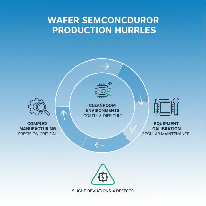
Wafer semiconductors play a crucial role in our technology-driven lives. The manufacturing process of these wafers is intricate and requires precision. One key step is the process of crystal growth. Silicon ingots are carefully formed. Once solidified, they are sliced into thin wafers. This step needs meticulous attention to produce smooth and uniform surfaces.
Another important phase is photolithography. A light-sensitive material is applied to the wafer. Patterns are then etched onto the wafer using ultraviolet light. This stage demands accuracy to ensure that circuits align perfectly. It can be challenging to get it right every time. Minor errors can lead to significant issues in the final product.
Finally, doping is essential for modifying the electrical properties of the wafers. Impurities are added to silicon to create n-type or p-type materials. This adds complexity to the manufacturing process. Engineers often face difficulties in achieving the desired conductivity levels. Overcoming these obstacles requires continuous innovation and expertise. Each step reflects careful planning and execution, but it is a constant learning process.
Types of Wafer Semiconductors and Their Applications
Wafer semiconductors play a crucial role in modern electronics. They are the foundation for various devices and technologies. There are different types of wafer semiconductors, each tailored for specific applications. For instance, silicon wafers dominate the market, accounting for almost 90% of semiconductor sales in 2022. Their versatility supports everything from computers to smartphones.
Gallium nitride (GaN) and silicon carbide (SiC) are emerging players. GaN wafers are vital for high-frequency and high-power applications. The global GaN market is projected to grow at a CAGR of over 30% from 2023 to 2030. On the other hand, SiC excels in power electronics, boasting high efficiency. It is expected that SiC devices will report a market size of around $6 billion by 2026.
However, the production process is not without challenges. Yield issues can arise during fabrication. More research is necessary to improve efficiency. The environmental impact of wafer manufacturing is also a topic for reflection. Creating sustainable practices remains a priority for the industry. As technology advances, the demand for optimized wafer semiconductors continues to grow. Balancing innovation with responsible practices is key.
Future Trends in Wafer Semiconductor Technology
Wafer semiconductor technology is poised for exciting advancements. Future trends suggest that we will see smaller, more efficient chips. Innovations in materials, like silicon carbide, are gaining traction. These materials promise better performance in extreme conditions. Emerging 5G technology will drive the need for higher-frequency devices. More manufacturers are exploring advanced packaging techniques to increase efficiency.
However, challenges remain. The demand for miniaturization can lead to overheating issues. This raises questions about long-term reliability. As chips get smaller, the risk of defects increases. These imperfections can affect overall performance. Companies must focus on quality control to meet expectations.
Research into quantum computing will also impact wafer technology. As scientists explore qubits, traditional designs may shift. This could redefine the future of processing power. Yet, integrating quantum solutions is complex. The industry needs to adapt quickly to these advancements. Balancing innovation with practicality will be crucial in the coming years.