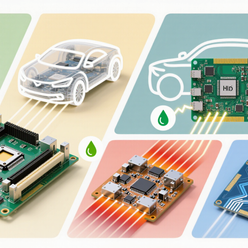
In 2026, pcb manufacturing is no longer defined by one dominant board type. Product designers now balance density, flexibility, thermal performance, signal integrity, and production yield. A wearable device may require a flexible PCB, while an artificial intelligence server can depend on HDI boards, advanced rigid designs, and high-layer-count structures. Electric vehicles add another challenge. Their boards must withstand heat, vibration, moisture, and continuous electrical load.
Dr. Hayao Nakahara, a respected PCB industry analyst, once observed, “The PCB is the foundation of every electronic product.” That foundation is becoming more complex. Rigid PCBs remain widely used because they offer stable performance and efficient large-scale production. Flexible and rigid-flex PCBs reduce wiring space, but their materials and assembly processes demand tighter control. HDI PCBs support compact components and shorter signal paths. High-frequency boards require carefully selected laminates and controlled impedance. Metal-core PCBs help move heat away from power components.
Small details matter.
A poorly aligned microvia can reduce reliability. Excessive copper density can complicate etching and warpage control. These risks are easy to underestimate. No manufacturing type is automatically the best choice. The correct solution depends on application requirements, supplier capability, testing standards, and total production volume. This overview examines the leading PCB manufacturing types shaping 2026. It also considers where industry assumptions may fail, because lower size, higher speed, and lower cost rarely arrive together.
Single- and double-sided PCBs remain practical choices when circuit density is moderate and cost control matters. Prismark’s 2024 market forecast valued global PCB production at approximately US$74 billion. That scale reflects continuing demand for simpler board structures.
Single-sided boards use copper on one surface. Double-sided boards add copper on the opposite surface, enabling more routing without a full multilayer stack-up. Fewer copper layers usually reduce lamination, drilling, material, and inspection requirements. IPC-2221 design guidance still supports these structures for many low-to-medium complexity applications. Keep traces visible. Keep manufacturing predictable.
In production, a double-sided board can often provide a useful middle ground. It supports plated through-holes, grounding paths, and compact component placement. However, “cheaper” is not automatic. A crowded two-layer layout may require narrow traces, tighter spacing, or extra jumpers. Those choices can increase scrap and testing time. IPC’s 2024 electronics industry data continues to highlight cost pressure and supply-chain risk across PCB production, making design-for-manufacturing important.
A practical review should check copper weight, minimum drill size, solder-mask clearance, and panel utilization. For example, 35-micrometre copper is common, but higher current may require thicker copper and wider tracks. That changes cost quickly. The imperfect part is easy to miss: a single-sided board may look cheapest, yet assembly can become slower and less reliable. A double-sided design may cost slightly more upfront but save space and labor.
Multilayer PCBs, typically ranging from 4 to 40+ layers, are becoming central to high-density electronics in 2026. They fit processors, memory, power delivery, and high-speed interfaces into compact products. Prismark’s 2024 worldwide PCB market forecast valued total industry revenue near USD 89 billion, with multilayer boards representing one of the largest technology segments. Demand is also supported by advanced computing, automotive electronics, and communication infrastructure.
Each layer adds routing capacity, but it also increases manufacturing risk. A four-layer board may use standard through-holes, while a 20-layer design often needs controlled impedance, sequential lamination, microvias, and tightly registered dielectric materials. IPC design and fabrication guidance emphasizes trace geometry, copper balance, and process control because small registration errors can damage signal integrity. In production reviews, engineers often find that an attractive layout fails during drilling or lamination. That lesson remains expensive.
High-layer-count boards require more than schematic accuracy. Fabricators must control resin flow, thermal expansion, warpage, and via reliability across the complete stack-up. The 2024 electronics industry outlook from IPC linked electronics growth with continuing investment in high-performance computing and infrastructure, areas that commonly use dense multilayer assemblies. Still, 40-layer capability does not automatically mean better engineering. Unused layers add cost, inspection time, and failure opportunities. A practical design may need fewer layers, but stronger power planes and cleaner routing.
Typical multilayer PCB layer counts increase as products require greater routing density, power integrity, signal isolation, and mechanical integration. The values below represent common engineering stackup levels rather than company-specific manufacturing data.
Layer counts are representative design points. Actual requirements depend on component density, controlled-impedance routing, power distribution, thermal design, HDI technology, and manufacturing constraints.
In 2026, HDI PCBs remain a leading choice for compact electronic designs. Their defining feature is high-density routing with microvias measuring 150 μm or less. These tiny interconnections shorten signal paths and release valuable surface area for processors, sensors, and wireless modules. They also support thinner boards without sacrificing essential routing capacity.
Small geometry creates serious process demands. Manufacturers typically use laser drilling, sequential lamination, and controlled copper filling. Each layer must align accurately, especially when several build-up cycles are required. Engineers should inspect microvia diameter, depth, copper coverage, and interlayer registration. Automated optical inspection helps, but it cannot replace cross-section analysis during process validation. A polished sample may look excellent while hidden voids remain inside the copper.
Thermal cycling is another practical concern. Compact microvias can experience stress from repeated heating and cooling. Material selection, resin flow, copper thickness, and via stacking therefore require careful coordination. Stacked microvias save space, yet staggered structures may offer better reliability in demanding applications. The smallest design is not automatically the best design. In production trials, a slightly wider feature can improve yield and reduce rework. This is where engineering judgment matters. Designers should balance density, current capacity, assembly tolerances, and inspection cost before approving a 2026 HDI layout. Mistakes become expensive when they are discovered after full-volume fabrication.
Flexible PCBs use polyimide film as a thin, heat-resistant substrate. Their copper traces fold through hinges, joints, and compact moving assemblies. This makes them valuable in 2026, when designers demand smaller electronics and fewer wire connections. A repeated-bend circuit is not simply a rigid board made thinner. Its copper type, layer stack, bend radius, and adhesive system must match the motion profile. Dynamic flex designs need controlled movement, not random creasing. Small details matter here.
During engineering reviews, I look for the actual bend path first. A circuit bending around a 5 mm radius may fail quickly if its copper is too rigid. Rolled-annealed copper usually tolerates repeated flexing better than harder alternatives. Designers should keep vias and solder joints away from the active bend zone. Stiffeners can support connectors, but they must end before the flexing area. Thermal cycling, vibration, and assembly pressure also deserve testing. No design is perfect. Early prototypes sometimes reveal unexpected crease points that drawings miss.
Tips: Define bend cycles before layout begins. Measure the minimum radius under real motion. Add strain relief near connectors. Use gradual trace transitions, not sharp corners. Ask the fabricator for cross-section details and test data. I would also inspect the first samples after repeated cycling, because a passing visual check proves very little.
What Are the Top PCB Manufacturing Types in 2026?
Rigid-flex PCBs combine rigid FR-4 sections with flexible polyimide zones. This structure supports three-dimensional electronic packaging. A board can fold around a battery, camera, or compact connector. It also removes several cable assemblies and solder joints. The trade-off is real. A 2024 Fortune Business Insights report valued the flexible PCB market at USD 28.17 billion. Its forecast shows strong growth through 2032. Estimates vary by market definition, so buyers should check the methodology.
Manufacturing begins with a controlled stack-up, not the artwork alone. Engineers must define bend zones, minimum bend radius, copper thickness, and coverlay openings. IPC-2223 guidance helps evaluate flexible and rigid-flex constructions. In production, laser drilling, sequential lamination, and controlled-depth routing can protect the transition area. FR-4 adds stiffness, but abrupt material changes can increase stress. Smooth pad edges matter. Tiny details matter more.
Thermal cycling exposes weak designs quickly. IPC’s 2024 technology roadmap continues to identify miniaturization, density, and reliability as major industry pressures. Prototype testing should include repeated bending, connector insertion, humidity, and temperature cycling. A 0.15-millimeter copper layer may suit one flex zone but fail another. That judgment needs measured evidence. Designers sometimes overvalue compactness. This remains a design weakness.
Key design and manufacturing characteristics of rigid-flex printed circuit boards using rigid FR-4 sections and flexible polyimide-based zones.
| Dimension | Rigid Section | Flexible Zone | Rigid-Flex Integration | Design and Manufacturing Relevance |
|---|---|---|---|---|
| Primary substrate | FR-4 glass-reinforced epoxy laminate | Polyimide film with flexible copper foil | Rigid and flexible materials are laminated into one interconnected structure | Material transitions must be controlled to prevent cracking, delamination, and impedance discontinuities |
| Mechanical function | Provides structural support and component mounting surfaces | Allows folding, bending, or limited dynamic movement | Supports three-dimensional packaging without separate wire harnesses or board-to-board connectors | Useful when electronics must fit around corners, inside compact enclosures, or across moving assemblies |
| Typical layer construction | Commonly 2 to 16 or more copper layers, depending on circuit density | Commonly 1 to 4 copper layers in flexible areas, although higher counts are possible | Layer counts may vary between rigid and flexible regions within the same board | Stack-up planning is required to balance routing density, flexibility, manufacturability, and cost |
| Copper type | Electrodeposited or rolled copper foil | Rolled-annealed copper is commonly preferred for repeated flexing; electrodeposited copper may suit static bends | Different copper choices can be used for rigid and flexible requirements | Copper grain structure and foil thickness affect bend life and resistance to fatigue |
| Bend capability | Designed to remain substantially flat after assembly | Can be bent around a defined radius when the bend area is properly designed | Flex zones enable controlled three-dimensional assembly while rigid zones remain stable | Minimum bend radius depends on layer count, copper thickness, coverlay construction, and whether bending is static or dynamic |
| Indicative bend-radius guideline | Not intended for repeated bending | Static bends are often designed around approximately 6–10 times the finished flexible thickness; dynamic bends generally require a larger radius | Rigid-to-flex transitions should not be placed directly in the highest-stress bend region | Actual values must be verified with the fabricator and the applicable design standard because construction details change the limit |
| Surface protection | Solder mask is normally applied over exposed circuitry | Flexible coverlay or flexible solder mask protects conductors while preserving bendability | Different protection systems may meet at the rigid-flex boundary | Coverlay openings, adhesive flow, and transition geometry influence reliability and assembly yield |
| Component mounting | Suitable for surface-mount and through-hole components | Surface-mount components are generally placed in supported, non-bending areas | Components can be mounted on rigid islands connected by folded flex sections | Heavy components and connectors should be mechanically supported and kept away from active bend zones |
| Thermal performance | Provides more stable mechanical support for thermal vias, copper planes, and heat spreaders | Has less thermal mass and may have limited space for large copper planes | Heat-generating components are typically concentrated on rigid sections | Thermal paths should be evaluated across material transitions and constrained enclosure spaces |
| Electrical performance | Supports controlled-impedance routing with defined dielectric thicknesses and reference planes | Controlled impedance is possible but requires tighter control of stack-up, coverlay, and bend geometry | Signal paths can pass continuously through rigid and flexible regions | High-speed designs should account for dielectric variation, copper roughness, vias, and discontinuities at transitions |
| Interconnection method | Plated through-holes, blind or buried vias, and surface-mount pads | Microvias, plated vias, and flexible-compatible copper features | Integrated transitions eliminate many detachable connectors and cable interfaces | Fewer interconnects can reduce assembly complexity, but rigid-flex fabrication requires more specialized process control |
| Dimensional stability | Generally stable because of glass reinforcement | More sensitive to moisture, temperature, handling, and lamination movement | Different coefficients of thermal expansion must be managed across the combined construction | Registration tolerances and material shrinkage should be considered during artwork and tooling development |
| 3D packaging benefit | Creates precise mounting platforms for components and mechanical attachment points | Routes signals through folds and constrained spatial paths | Enables compact folded assemblies with fewer cables and connectors | Can reduce package volume and improve assembly repeatability when the bend sequence is well defined |
| Main reliability risks | Thermal stress, via fatigue, delamination, and solder-joint failure | Copper fatigue, conductor cracking, coverlay damage, and flex-zone delamination | Stress concentration at rigid-to-flex transitions and improper bend handling | Gradual transition geometry, adequate stiffeners, tear-drop features, and bend-radius control improve durability |
| Inspection focus | Automated optical inspection, electrical testing, and X-ray inspection where appropriate | Visual inspection of coverlay, conductor edges, bend areas, and exposed adhesive | Registration, layer alignment, transition quality, and mechanical fit must be checked together | Testing should reflect the final folded shape and the expected static or dynamic bending condition |
| Best-fit applications | Control boards, sensor modules, power-management sections, and connector support areas | Wearable devices, compact sensors, camera modules, medical instruments, and moving mechanisms | Avionics, automotive electronics, industrial controls, robotics, and compact consumer assemblies | Selection is strongest when space savings, reduced wiring, and reliable 3D integration justify added fabrication complexity |
| Cost considerations | Usually lower-cost and easier to source than a comparable rigid-flex design | Material and processing costs are generally higher than standard rigid PCB construction | Higher initial fabrication cost may be offset by fewer connectors, cables, assembly steps, and field failure points | Total cost should include tooling, assembly, testing, mechanical integration, and expected lifecycle reliability |
| Recommended design documentation | Layer stack-up, drill table, impedance requirements, solder-mask data, and assembly drawings | Bend zones, bend direction, minimum radius, coverlay openings, stiffener locations, and no-component zones | Flat-pattern drawing plus formed-state drawing and a defined folding sequence | Clear documentation reduces ambiguity between electrical, mechanical, fabrication, and assembly teams |
Note: Ranges and guidelines are general engineering references. Final material selection, stack-up, bend radius, tolerances, and qualification tests should be confirmed against the applicable IPC requirements, product environment, and fabricator capabilities.