Understanding the Semiconductor Process and Its Impact on Technology Development
The semiconductor process is a cornerstone of modern technology development, transforming a multitude of industries and everyday applications. As electronic devices become more integrated and sophisticated, understanding the intricacies of the semiconductor process has never been more critical. This process involves several complex stages, including the fabrication, testing, and packaging of semiconductor chips, which serve as the brains behind everything from smartphones to advanced computing systems.
With rapid advancements in technology, innovations in semiconductor manufacturing have had profound implications for performance, efficiency, and cost-effectiveness. As we delve deeper into the impact of the semiconductor process on technological evolution, it becomes clear that even minor improvements in this field can lead to significant breakthroughs in areas such as artificial intelligence, internet of things (IoT), and renewable energy. By comprehensively examining the semiconductor process and its influence on technology development, we can better appreciate the delicate interplay between engineering, manufacturing, and the future of digital transformation.

The Semiconductor Fabrication Process: An Overview of Key Steps
The semiconductor fabrication process is a complex journey that transforms raw materials into tiny chips that power our modern technology. This process generally consists of multiple key steps: photolithography, etching, doping, and packaging. In photolithography, light is used to transfer intricate patterns onto a semiconductor wafer, a crucial phase that determines the circuit design. According to a report by the Semiconductor Industry Association (SIA), advancements in photolithography techniques, such as extreme ultraviolet (EUV) lithography, are enabling manufacturers to produce chips with transistors as small as 2 nanometers, improving efficiency and performance significantly.
Following photolithography, etching removes unwanted material from the wafer to create the desired patterns. This is typically followed by doping, where impurities are introduced to modify the electrical properties of the semiconductor. As reported in McKinsey's Semiconductor Sector Report, the doping process is vital for optimizing performance, particularly in high-frequency applications where precision is critical. Finally, the packaging of chips represents the last step in this intricate process, ensuring that the delicate semiconductors are protected and can efficiently connect with other electronic system components. The continuous evolution of these stages will not only enhance semiconductor efficiency but also bolster innovations in various technology sectors, ranging from consumer electronics to artificial intelligence and beyond.
Understanding the Semiconductor Process and Its Impact on Technology Development
| Step in Semiconductor Fabrication |
Description |
Impact on Technology Development |
| Wafer Cleaning |
Removing contaminants from the wafer surface to ensure proper adhesion and quality of layers. |
Improves precision in fabrication, reducing defects that could lead to device failure. |
| Oxidation |
Growing an oxide layer on the silicon wafer to form a dielectric layer for insulation. |
Enables miniaturization of components and enhances electrical isolation in devices. |
| Photolithography |
Using light to transfer geometric patterns onto the wafer. |
Critical for defining circuit patterns, greatly impacting circuit density and performance. |
| Etching |
Removing material from the wafer to create desired patterns after photolithography. |
Allows for the formation of complex circuit designs, essential for advanced electronics. |
| Doping |
Introducing impurities into the semiconductor to modify its electrical properties. |
Enhances the efficiency and functionality of semiconductor devices by creating p-type and n-type materials. |
| Metal Deposition |
Depositing metal layers for electrical connections between components. |
Critical for ensuring low resistance contacts, improving device speed and performance. |
| Packaging |
Enclosing the semiconductor device to protect it while allowing electrical connections. |
Essential for device usability, impacting heat dissipation and mechanical integrity. |
Critical Role of Doping and Ion Implantation in Semiconductor Performance
Doping and ion implantation are critical processes in the semiconductor manufacturing landscape, significantly influencing the performance characteristics of silicon-based devices. Doping involves introducing impurities into the semiconductor to modify its electrical properties, thereby enhancing conductivity. According to the Semiconductor Industry Association, doping techniques can improve carrier concentration, effectively increasing the performance of transistors and other semiconductor components. For instance, careful control over doping levels can lead to a reduction in threshold voltage, which directly impacts device speed and power consumption.
Ion implantation, on the other hand, allows for precise control over the location and concentration of dopants within a semiconductor material. This technique has become increasingly indispensable, especially as the industry moves towards smaller geometries. Reports from leading market analysts project that advanced ion implantation systems can achieve doping accuracies within a few nanometers, which is essential for maintaining the integrity of electronic circuits as transistor sizes shrink below 5 nanometers. As devices become more compact and complex, the role of ion implantation in ensuring consistent semiconductor performance cannot be overstated, solidifying its position as a cornerstone technology in the ongoing evolution of electronic devices across various applications.
Impact of Doping Concentration on Carrier Concentration in Semiconductors
This chart illustrates the relationship between doping concentration and carrier concentration in semiconductors. As the doping concentration increases, the carrier concentration also rises significantly, which is crucial for enhancing semiconductor performance and influencing technology development.
Advancements in Photolithography Technologies and Their Impact on miniaturization
Photolithography technologies play a crucial role in the semiconductor manufacturing process, driving the ongoing trend of miniaturization in electronic devices. The advancement of photolithography involves the use of light to project intricate circuit designs onto silicon wafers, enabling the production of smaller and more complex semiconductor components. As the demand for more powerful and efficient devices grows, innovations such as extreme ultraviolet (EUV) lithography have emerged, significantly enhancing the resolution and precision of patterning at nanoscale dimensions.
These advancements have a profound impact on technology development, allowing for the integration of more transistors into a single chip. This not only increases computational power but also improves energy efficiency, a critical factor in today's mobile and IoT devices. Furthermore, with the ability to develop smaller chips, manufacturers can explore new materials and designs that were previously impractical, thus setting the stage for breakthroughs in areas such as artificial intelligence, advanced telecommunications, and high-performance computing. As photolithography continues to evolve, its influence on the semiconductor industry remains a key driver of technological progress.
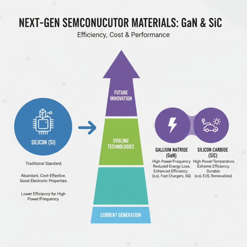
The Influence of Semiconductor Materials on Device Efficiency and Cost
The efficiency and cost of semiconductor devices significantly hinge on the materials used in their production. Silicon has long been the standard semiconductor material due to its favorable electronic properties and abundant availability. However, as the demand for higher efficiency and lower power consumption grows, alternative materials like gallium nitride (GaN) and silicon carbide (SiC) are gaining traction. These materials not only offer improved performance for high-power and high-frequency applications but also contribute to reduced energy losses, thus enhancing overall device efficiency.
Tips: When considering the choice of semiconductor materials, it’s essential to weigh the trade-offs between performance and manufacturing costs. For applications requiring extreme efficiency, investing in advanced materials like GaN or SiC might lead to long-term savings despite higher initial costs. Additionally, staying informed about emerging materials science research can provide insights into potential innovations that may disrupt current market standards.
Furthermore, the development process of semiconductor components directly influences their cost-effectiveness. Innovations in fabrication techniques, such as atomic layer deposition and advanced lithography, enable the production of smaller and more efficient devices. As manufacturing methods improve, they allow for more complex structures and functionalities without significantly raising production costs. This ongoing evolution is critical for maintaining competitiveness in a rapidly advancing technological landscape.
Tips: Keeping an eye on advancements in semiconductor manufacturing processes can help businesses adapt and optimize their production strategies. Engaging in collaborations with research institutions can also pave the way for accessing cutting-edge technologies, fostering innovation, and enhancing overall product performance.
Future Trends in Semiconductor Manufacturing and Their Technological Implications
The semiconductor manufacturing industry is on the cusp of significant transformation, driven by advancements in technology and shifting market demands. With the global semiconductor market projected to reach $1 trillion by 2030, as reported by industry analysts, this growth underscores the critical role these components play across various sectors, including automotive, telecommunications, and consumer electronics. Future trends indicate a move towards smaller, more efficient transistors, with many companies achieving successful 3nm processes which promise higher performance while consuming less power.
As developments continue, it’s crucial to consider the implications of these advancements. Emerging technologies such as AI and 5G are expected to drive the need for advanced semiconductor materials. The adoption of silicon carbide and gallium nitride can enable better performance in high-voltage devices, with the power semiconductor market projected to grow at a CAGR of 10.5% through 2026. This shift not only enhances device efficiency but also contributes to sustainability initiatives by reducing energy consumption.
Tips: As a professional navigating this fast-evolving landscape, staying informed about new manufacturing techniques and materials is key. Attend industry workshops and webinars, read research from reputable organizations, and network with specialists to gain insights into how these trends can impact your field. Embracing these innovations early can position you ahead of the curve in this competitive industry.