What are the key steps in the semiconductor process?
The semiconductor process is a complex journey that transforms raw materials into essential components for modern technology. Renowned expert Dr. Lisa Chen from Tech Innovations once stated, “Every step in the semiconductor process is critical; a single flaw can disrupt the entire chain.” This highlights the importance of precision throughout the process.
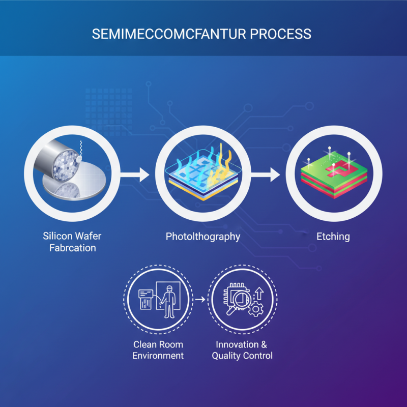
In the semiconductor process, several key steps must be meticulously followed. They include silicon wafer fabrication, photolithography, and etching. Each step requires advanced technology and skilled professionals. The fabrications start with pure silicon, which is then cut into wafers. Next, layers of materials are added and shaped using light exposure. These actions may seem routine, yet any oversight can lead to significant production issues.
Moreover, the semiconductor process involves numerous challenges. For example, the need for clean rooms to prevent contamination adds complexity and cost. While progress has been made, constant advancements are necessary to meet expanding demands in electronics. It is clear that balance between innovation and error prevention remains an ongoing conversation in the industry.
Overview of Semiconductor Fabrication Processes and Technologies
The semiconductor fabrication process involves several intricate steps. Each step plays a crucial role in creating advanced electronic components. These components are foundational to modern technology.
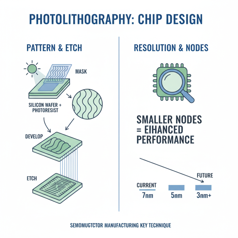
Photolithography is one of the key processes. It transfers patterns onto semiconductor wafers. A photoresist material is applied. Light exposure changes its properties, allowing selective etching.
Etching and doping follow, essential for forming the desired circuitry. In etching, parts of the wafer are removed to create intricate designs. Doping introduces impurities into the semiconductor. This alters its electrical properties, enabling functionality.
Another important stage is oxidation, which forms a protective layer. It can enhance the performance and longevity of the devices.
However, challenges persist. Many parameters must be carefully controlled. Contaminants can ruin a batch, leading to waste. Ensuring uniformity is difficult but critical. Equipment maintenance is also a constant concern. Reflection on these practical issues can lead to better practices. The world of semiconductor fabrication remains complex and ever-evolving. Each step requires precision and expertise in an ever-demanding field.
Silicon Wafer Preparation: Cleaning, Slicing, and Polishing Techniques
The process of semiconductor fabrication begins with silicon wafer preparation. This fundamental step includes cleaning, slicing, and polishing techniques. The quality of the wafer significantly influences the overall performance of the semiconductor devices produced. A clean wafer is essential to minimize defects and improve yield.
Cleaning typically involves both physical and chemical methods. Various cleaning agents help remove organic contaminants and particulates. Data suggests that improper cleaning can lead to defects, affecting up to 30% of the final product yield. This highlights the need for rigorous cleaning protocols.
Once the cleaning is completed, slicing the silicon ingot into thin wafers follows. The precision of this cut is critical. It typically ranges between 150mm and 300mm in diameter. Studies show that a 1mm error in slicing can result in significant material waste. Finally, polishing is necessary to achieve the desired surface roughness. Even minor imperfections can lead to performance issues in subsequent processes. Investing in high-quality polishing techniques can elevate performance, although the costs must be justified by the improved outcomes.
Silicon Wafer Preparation Process Steps
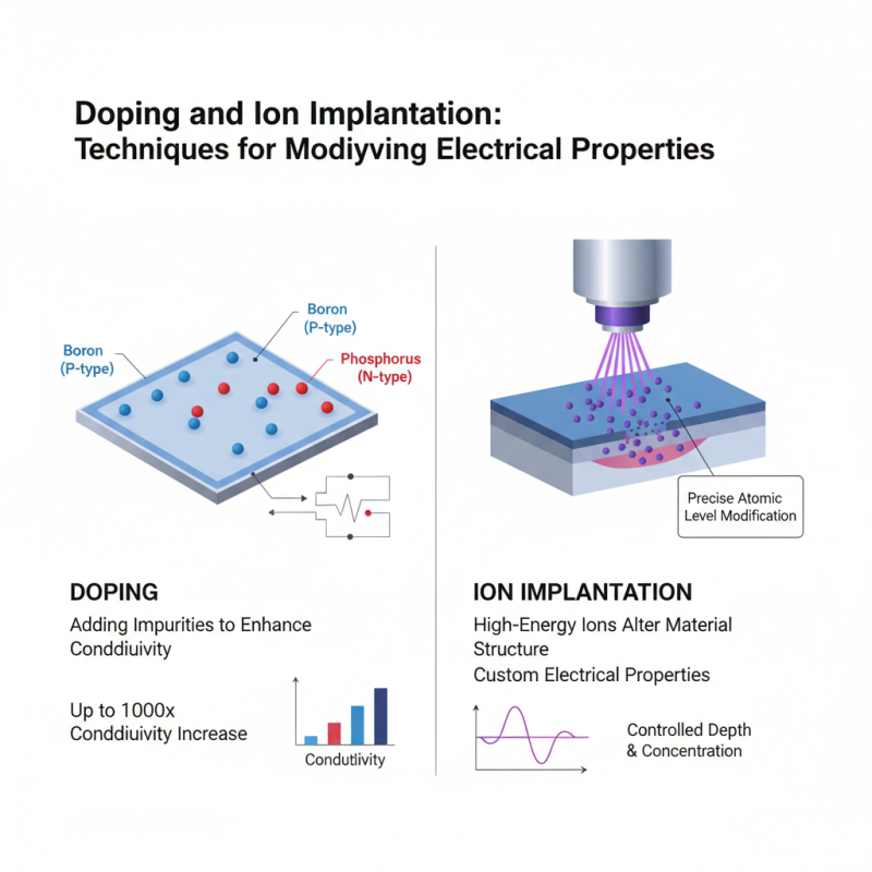
Doping and Ion Implantation: Techniques for Modifying Electrical Properties
Doping and ion implantation are crucial techniques in semiconductor manufacturing. These processes modify the electrical properties of silicon and other materials. In the doping process, impurities are added to semiconductors to enhance conductivity. Phosphorus and boron are common dopants, each imparting unique electrical qualities. Reports show that proper doping can increase conductivity by up to a thousand times.
Ion implantation differs from traditional doping. It fires ions into the semiconductor substrate at high speeds. This precision allows for control over the depth and concentration of dopants. According to industry studies, ion implantation can provide better uniformity compared to diffusion techniques. However, implementing these techniques can be challenging. There is a risk of damage to the crystal structure during implantation. Balancing dosage and energy is critical.
Moreover, there are limits to how effectively these techniques can be applied. As feature sizes shrink, achieving the desired doping profiles becomes difficult. The semiconductor industry's shift to advanced nodes has made ion implantation even more complex. Ongoing innovation is needed to address these challenges, ensuring efficiency in future semiconductor devices.
Testing and Packaging: Ensuring Quality and Performance in Semiconductors
In the semiconductor process, testing and packaging play crucial roles. After fabrication, chips require thorough testing. This step identifies defects that could affect performance. Without proper testing, faulty semiconductors can lead to significant failures in devices.
One common method of testing is functional testing. It checks if the semiconductor meets design specifications. Engineers also conduct stress tests. These simulate extreme conditions to see how components behave. It's essential to document any anomalies during these tests. This documentation can drive future improvements.
Packaging comes next. It's not just about physical protection. The right package improves heat dissipation and ensures electrical connectivity. A well-designed package can enhance performance. However, creating a perfect package is challenging. Sometimes, compromises must be made. This requires careful consideration of priorities.
Tips: Ensure thorough documentation during testing. It helps in analyzing trends and improving the process. Always analyze the packaging materials. They should match the application requirements for optimal performance. Reflection on past failures can be valuable for innovation.
Key Steps in the Semiconductor Process: Testing and Packaging
| Step |
Description |
Importance |
| Wafer Testing |
Initial tests to check for defects at the wafer level. |
Identifies quality issues early and reduces waste. |
| Die Preparation |
Dicing the wafer into individual chips for further testing. |
Prepares chips for functional and performance testing. |
| Functional Testing |
Tests each die's functionality against specifications. |
Ensures reliability and meets performance criteria. |
| Sorting and Binning |
Classifies dies based on performance and quality metrics. |
Optimizes performance per application requirements. |
| Packaging |
Encapsulation of dies to protect them during usage. |
Ensures physical protection and thermal management. |
| Final Testing |
Comprehensive tests including stress, reliability, and performance. |
Validates packaged product before shipment to ensure quality. |