Choosing the right semiconductor process is a technical decision with long-term consequences. It affects performance, power consumption, manufacturing cost, yield, and product lifetime. A suitable process begins with the product, not with the newest technology node.
Engineers should define measurable requirements before comparing foundries or process platforms. These requirements may include clock speed, leakage current, operating temperature, wafer size, and expected production volume. For example, a battery-powered sensor may benefit more from low leakage than extreme transistor density. A high-performance processor may require advanced FinFET or gate-all-around technology. The correct semiconductor process depends on trade-offs.
Practical evaluation should combine simulation, foundry documentation, pilot wafers, and reliability data. Review design rules carefully. Check available IP, packaging options, process maturity, and statistical process control results. A mature node can deliver better yield and shorter qualification time. An advanced node may provide stronger performance, but it often demands higher design costs and tighter manufacturing control.
Real projects rarely offer a perfect answer. Early estimates can miss thermal issues or packaging limits. That deserves attention. Teams should challenge optimistic assumptions with small prototype runs and independent reviews. Lessons from previous tape-outs are valuable, even when they reveal uncomfortable mistakes. A reliable choice balances technical ambition with production evidence, supplier capability, and the product’s actual market needs. This guide explains how to compare each factor and select a semiconductor process with greater confidence.
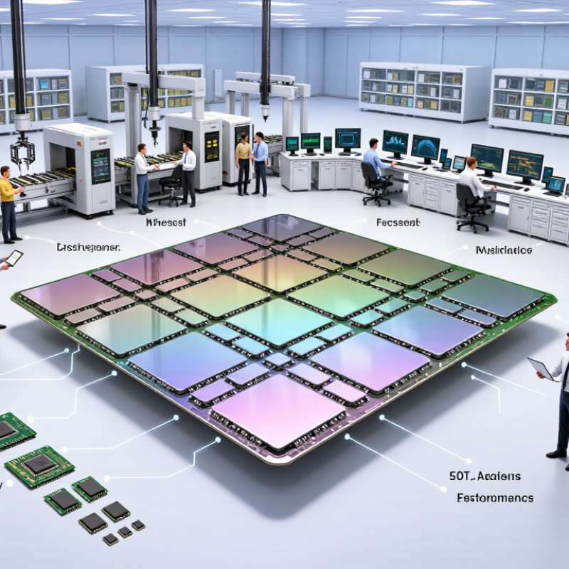
Defining the application is the practical starting point for process selection. A process should serve the product, not impress the design team. In engineering reviews, I begin with operating voltage, signal frequency, temperature range, package size, and expected production volume. A battery-powered sensor may value leakage control more than peak speed. A high-frequency interface may need tighter parasitic control. Not every design needs the smallest feature size.
Performance requirements must be measurable. Replace “fast” with a target such as a 2-nanosecond response time. Specify standby current, noise limits, accuracy, operating lifetime, and thermal resistance. Include real conditions, such as a 70°C enclosure or a weak supply rail. Datasheets provide useful boundaries, but application tests reveal interactions that simulations can miss. Early prototypes should measure startup behavior, heat distribution, signal integrity, and process variation.
I once focused too heavily on maximum transistor speed and underestimated power density. The circuit met its laboratory target, but the enclosed board became unexpectedly hot. That result changed the evaluation method. Now, I compare typical and worst-case data before approving a process direction. The review also includes yield assumptions, available design rules, and long-term reliability evidence.
These details can expose uncomfortable trade-offs. Reality is often less elegant. A slower process may deliver better stability, easier qualification, and more predictable manufacturing costs.
How to Choose the Right Semiconductor Process?
Comparing Semiconductor Process Technologies
Choosing a semiconductor process starts with the product, not the smallest advertised feature size. A battery-powered sensor may value leakage control more than peak speed. A data-processing device may need dense logic and fast interconnects. These goals can point to different technologies.
Mature planar processes often provide stable yields, lower mask costs, and strong support for analog functions. They suit power management, control circuits, and industrial interfaces. More advanced FinFET or gate-all-around processes improve transistor density and switching efficiency. However, they usually increase design complexity, verification time, and manufacturing expense. Smaller dimensions do not automatically produce a better chip.
Engineers should compare power, performance, area, yield, reliability, and total development cost. Test structures can reveal leakage, threshold variation, and metal resistance before full production. Packaging also matters. A modest process with effective thermal design may outperform a newer process in the field. That detail is easy to miss.
In practical evaluations, memory requirements often change the decision. Embedded memory, high-voltage devices, and radio-frequency blocks may need specialized process options. Design teams should review manufacturing data, not rely only on simulations. Simulation can look excellent. Silicon can disagree.
I once underestimated the impact of interconnect delay in a dense design. The transistor speed was impressive, but routing consumed the expected advantage. That experience supports a cautious comparison: evaluate the complete system, including package, software workload, testing, and expected production volume. The best choice is sometimes less advanced, and that can feel uncomfortable.
| Process Technology Class | Typical Transistor Structure | Typical Supply Voltage | Relative Density | Performance Potential | Power Efficiency | Manufacturing Cost | Common Application Areas | Best Selection Scenario |
|---|---|---|---|---|---|---|---|---|
| 180–130 nm | Planar CMOS | Approximately 1.8–3.3 V | Low | Low to moderate | Moderate, with strong tolerance for high-voltage designs | Low | Power management, display drivers, sensors, industrial controllers | When long product life, low mask cost, or higher operating voltage is more important than density |
| 90–65 nm | Planar CMOS | Approximately 1.0–1.8 V | Low to medium | Moderate | Moderate | Low to moderate | Connectivity devices, embedded controllers, automotive electronics, mixed-signal products | When mature design libraries, analog capability, and predictable supply are required |
| 45–40 nm | Planar CMOS, often with improved gate-stack materials | Approximately 0.9–1.2 V | Medium | Moderate to high | Good for cost-sensitive digital systems | Moderate | Consumer processors, communication chips, image processing, embedded systems | When a balance of performance, design maturity, and manufacturing cost is needed |
| 28 nm | Planar CMOS with multiple process variants | Approximately 0.8–1.1 V | Medium to high | High for many mainstream designs | Good | Moderate and generally lower than leading-edge nodes | Microcontrollers, networking, automotive control, industrial and consumer electronics | When proven production, broad intellectual-property support, and reasonable economics are priorities |
| 22–16 nm | FinFET | Approximately 0.7–1.0 V | High | High | Very good compared with older planar nodes | High | Advanced processors, graphics, networking, high-performance embedded systems | When high performance and improved leakage control justify greater design and mask complexity |
| 10–7 nm | FinFET with highly scaled interconnects | Approximately 0.6–0.9 V | Very high | Very high | Very good, although system-level power may remain high | Very high | High-performance computing, mobile processors, artificial-intelligence accelerators, advanced networking | When maximum compute density and energy efficiency are critical and the product volume supports high development cost |
| 5–3 nm | Gate-all-around or nanosheet transistor structures | Approximately 0.5–0.8 V | Extremely high | Extremely high | Excellent at the transistor level, subject to interconnect and packaging limits | Extremely high | Advanced computing, artificial intelligence, premium mobile systems, high-density system-on-chip designs | When performance per watt and maximum integration are more important than development cost and production complexity |
| Important note: Process-node names are industry labels rather than directly comparable physical gate lengths. Actual density, performance, power, yield, and cost depend on the specific process variant, design rules, interconnect stack, memory technology, packaging, operating conditions, and production volume. | ||||||||
Evaluating Materials, Features, and Manufacturing Constraints
Choosing a semiconductor process begins with the material, not the equipment list. Silicon supports mature manufacturing and broad design flexibility. Wide-bandgap materials can handle higher temperatures and voltages, but they often demand stricter defect control. The right option depends on operating conditions, target performance, and acceptable production risk.
Feature requirements must match process capability.
A narrow gate, deep trench, or dense memory array may require advanced lithography and tighter overlay control. These features increase inspection needs and can reduce yield when process variation grows. Engineers should compare electrical targets with realistic line widths, layer counts, and thermal budgets. Smaller is not automatically better.
Manufacturing constraints can change the decision. Check wafer availability, furnace temperature limits, contamination controls, and packaging compatibility. A process that works in a laboratory may fail during continuous production. Pilot runs should measure defect density, critical dimensions, leakage, and wafer-to-wafer variation. Data matters more than attractive simulations.
There is no perfect process.
In practice, teams sometimes overvalue feature size and undervalue equipment stability. I have seen a slightly older process deliver better results because operators understood its failure patterns. That choice may look less impressive on paper. Still, repeatable output, qualified materials, and manageable maintenance often protect the final product better than maximum density. Critical assumptions should remain open to challenge.
How to Choose the Right Semiconductor Process?
Balancing Cost, Yield, Power, and Long-Term Scalability
Choosing a semiconductor process starts with the product’s real workload, not a headline specification. A low-cost process may require more design effort, larger die area, or expensive packaging. Compare cost per good die, not wafer price alone. Yield matters early. Review defect maps, parametric distributions, and results across several wafer lots.
Power targets also need practical testing. Measure leakage during standby, switching power under realistic workloads, and heat at peak operation. A process with excellent speed may create thermal problems in a compact enclosure. Small gains can become expensive. Keep the test conditions visible. Otherwise, teams may compare numbers measured at different temperatures or voltages.
Long-term scalability deserves equal weight. Check available design rules, equipment capacity, memory options, and future node migration paths. Confirm that the process supports reliable packaging and supply continuity. I once overvalued performance data from a small pilot run. Later, yield variation changed the business case. That mistake was useful, but avoidable. Use staged prototypes, independent reliability checks, and clear stop criteria before committing. Some trade-offs hurt. The best choice is usually the process that remains predictable when volume, temperature, and product complexity increase.
Balancing cost, yield, power efficiency, and long-term scalability
The chart uses normalized industry benchmark scores, where a higher score is better. Mature nodes generally provide lower manufacturing cost and higher production stability, while advanced nodes offer better power efficiency and greater scaling potential at higher process complexity and development cost. The optimal choice depends on product volume, performance targets, reliability requirements, and expected product lifetime.
How to Choose the Right Semiconductor Process?
Selecting and Validating the Most Suitable Process Node
Choosing a process node starts with the product, not the smallest available geometry. Define the required speed, power budget, memory size, voltage range, and operating temperature. A sensor for industrial equipment may value long-term stability more than maximum density. A compact processor may need tighter performance margins. Each decision changes the process requirements.
Review the process design kit, device models, design rules, and available intellectual property. Check whether the models cover corners, mismatch, temperature, and aging effects. Then run early simulations with realistic parasitic estimates. A spreadsheet can look convincing and still be wrong. My early estimates were too optimistic when wiring resistance was treated as negligible.
Validation should include a small test structure or a multi-project wafer run when practical. Measure leakage, threshold variation, timing, thermal behavior, and defect patterns. Compare silicon data with pre-production simulations, not with ideal targets. Confirm wafer availability, packaging compatibility, qualification support, and expected yield. Ask how process changes are communicated. Document every assumption and its evidence. Keep a fallback node in the plan. It may cost more. That risk is often cheaper than redesigning the chip after fabrication.